Rolive

joined 2 years ago
[–] Rolive@discuss.tchncs.de 5 points 21 hours ago

That is very likely to be my next laptop.

[–] Rolive@discuss.tchncs.de 20 points 6 days ago (6 children)

Can't you get like, a diamond drill bit and just give it a light tap? Tempered glass breaks easily if the outside layer is compromised.

[–] Rolive@discuss.tchncs.de 16 points 1 week ago (1 children)

FreeCAD has improved drastically with the 1.0 update. There's no need to tolerate this corporate BS.

[–] Rolive@discuss.tchncs.de 6 points 1 week ago

Grachtengordel.

[–] Rolive@discuss.tchncs.de 2 points 1 week ago

TIL Ozzy is a witcher.

[–] Rolive@discuss.tchncs.de 2 points 1 week ago

It works as well with a 450nm diode laser. About 1W worth of laser power will ablate soldermask as well but you risk burning off really small pads because they cannot really dissipate heat anymore. Especially NC pads tend to burn off. I've tried it and it works reasonably well by doing the drilling as the last step.

450nm is unfortunately not good enough to cure soldermask, 405nm is much more effective.

25
submitted 1 week ago* (last edited 1 week ago) by Rolive@discuss.tchncs.de to c/electronics@discuss.tchncs.de
 

This is UV sensitive solder mask resin, applied as thin as possible using a silk screen mesh. Afterwards it's heated at about 90C for 10 minutes. This makes it more sensitive to UV light by evaporating most of the solvent.

It is exposed with a 405nm laser at about 250mw of power. I intentionally unfocused the laser for a spot size of about 0.5nm

After exposure the pads are easily cleaned off with some IPA.

[–] Rolive@discuss.tchncs.de 5 points 1 week ago (5 children)

Isn't wind energy better on balconies?

[–] Rolive@discuss.tchncs.de 2 points 1 week ago

Time to make the mother of all omelettes. Can't fret over every egg!

[–] Rolive@discuss.tchncs.de 1 points 1 week ago* (last edited 1 week ago)

I have different subfolders per project for it's components.

Project/KiCAD

Project/FreeCAD/Model1

Project/FreeCAD/Model2

Etc.

Each project has it's own set so it's easy to find. I think it's better than having all 3D printing related things together and then having to sort which project it belongs to.

[–] Rolive@discuss.tchncs.de 52 points 1 week ago* (last edited 1 week ago) (2 children)

Officer: Why were you speeding?

Me: Wanted to avoid ads.

[–] Rolive@discuss.tchncs.de 3 points 2 weeks ago

Generating bullshit is it's main feature.

[–] Rolive@discuss.tchncs.de 1 points 2 weeks ago

Interesting. I've been planning to build a flow battery for a while now just don't have the time.


I'm currently using an Orbiter 1.5 and it's pretty decent but I'm looking for an upgrade. I like the light style extruder sitting on the gantry over a Bowden system as it allows for flexible filament and has much better control over retraction.

Is the 2.0 a significant improvement over the 1.5? Should I get a new hotend as well with it?

Right now I'm using a MicroSwiss all metal hotend and am quite satisfied with it.

Print speed is okay I guess.


Hi all

I've made a detachable toolhead mod for an Ender 5 that uses an MGN12 linear rail on the X axis. It also assumes using an Orbiter 1.5 extruder. The idea is to be able to switch between 3D printing, lasercutting and very light milling easily. The main purpose is to be able to use the Ender 5 for PCB making and that is what the small drill unit is good enough for.

Let me know what you think and feel free to remix it for your own setup!


Hi all

Does anyone have any experience with this kit? I'm interested in the linear rail upgrade and CoreXY as well for higher printspeeds.

I sometimes attach a small PCB drill to my Ender5 to help with diy PCBs and may want to try basic CNC milling as well with it.

There are two kits for the Ender5, one for the Ender5 Pro and Ender5 Plus. The difference is in the size of the linear rails. Do the rails for the Ender5 Plus fit on the Ender5? On paper they are smaller than the size of the frame and in the future I might upgrade the Ender 5 to a bigger frame. I don´t mind if they stick out a little bit if it makes upgradability better.


Hi there

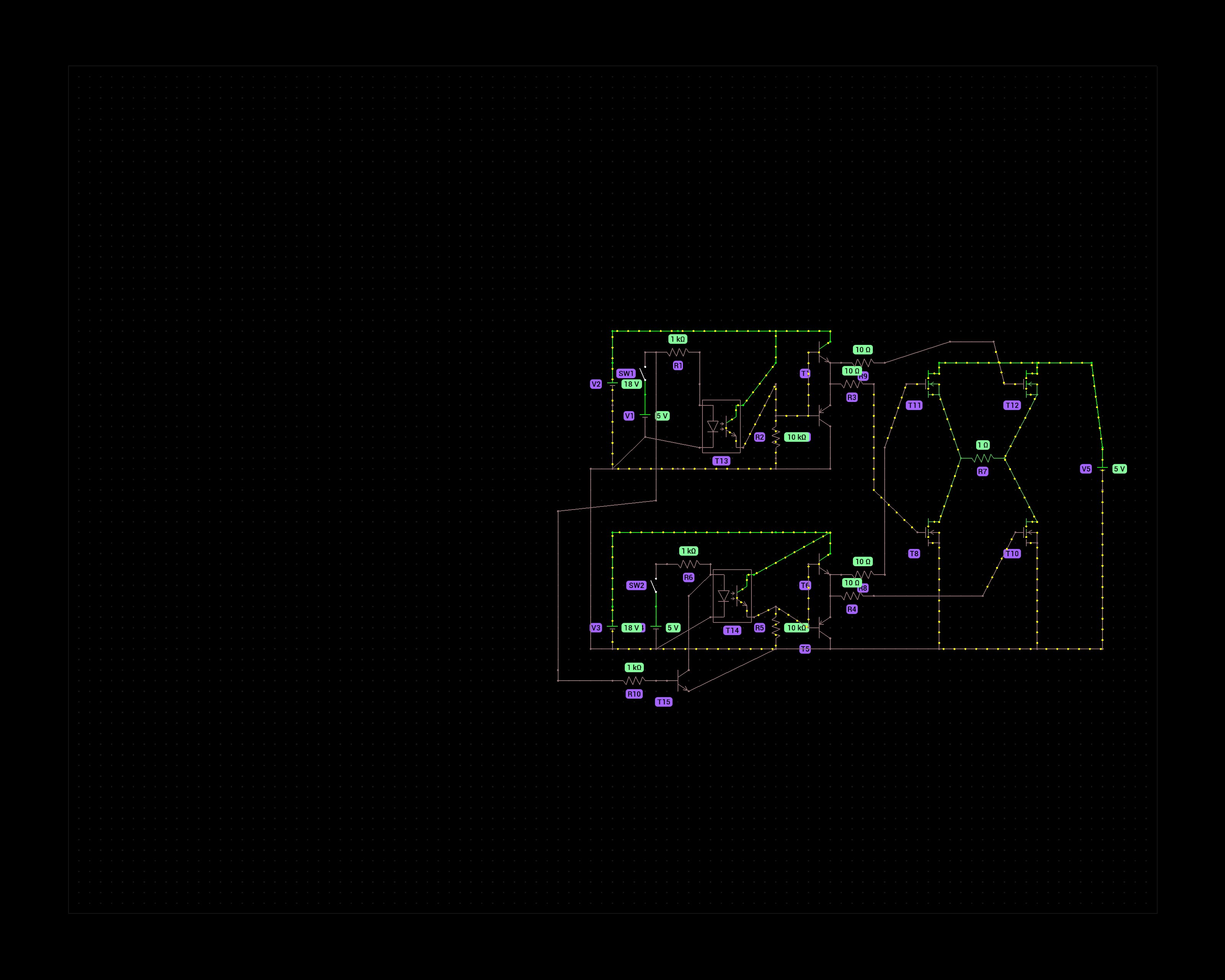
The purpose of this schematic is to control a DC motor that runs at 8V max. That is why I chose 4 N-channel mosfets in the H bridge. P-channels would not fully activate at voltages above -10Vgs but the N-channels can handle 18V at the gate.

The 5v switches represent an Arduino's digital output pins. One to turn forward, one for reverse. To prevent a failure scenario where both pins are HIGH I added a transistor that prevents current from flowing through the optocoupler on the second half bridge.

Does this circuit make sense? I'm not an electronics engineer, just a hobbyist and have doubts about how effective the gate driving circuit is of the mosfets.

Thanks!


According to the A4998 datasheet you're supposed to wait 1 millisecond after waking from sleep to allow the circuit to energise.

What is the worst that can happen if you neglect to do this? I use stepper motors to drive a plant watering pump and losing a step or two really isn't an issue. Is there a risk of damaging the module or is losing the first step the biggest risk?

I trigger the pump by pulling the EN pin low and a 555 timer on the STEP pin makes it pump continuously. It seems sensible to pull the SLP pin down as well with it as that saves a little bit of power.


Hi everyone

I've been experimenting with methods of applying etch resist with a laser and dry film. The process is kind of arduous and error prone.

Developing with sodium carbonate solution to clear unexposed etch resist takes long, doesn't work well and if you leave it too long the developed etch resist will break as well.

I use a laser module attached to a 3D printer to draw the PCB (LCB?) on the etch resist. This laser almost instantly solidifies toner for laserprinters and also almost instantly hardens dry film.

Using powdered toner and a laser would be a much quicker way to apply etch resist since the excess can be wiped off and reused easily. The problem is applying a uniform layer of toner.

Suspending toner on the surface of water and hydrodipping the plate seems to work but drying takes too long.

Spray coating could work but is messy.

Isopropyl alcohol softens the toner too much making it impossible to clean the excess off.

I have not tried using a roller or electrostatic application yet but that could work well.

Does any of you have experience with this and have ideas/advice?


LEDs will conduct more current when they get warmer and differences between individual LEDs mean you cannot easily put them in parallel. A constant current DC supply will be good enough for part of the LEDs but will overload some others. To normalize current a series resistor is used with each individual LED.

Now, those resistors waste a bit of power. Are they really necessary? If you put several LEDs in series the individual differences become negligible at some point and a constant current supply will suffice for several strips of series LEDs in parallel.

How many LEDs would this require? Another possibility would be to have the resistor in series with a strip of LEDs.

I got some LED strips off AliExpress that run on 12V and each individual LED has a resistor in series with it. I believe this to be quite wasteful and it would be better to have several LEDs in series with a current regulator instead. The LEDs will end up in an autonomous greenhouse where power efficiency is important.


This is an idea that entered my mind. The traditional way is applying some etch resist like toner or dry film, etching away the copper and then adding solder mask before populating the board with components.

Can the solder mask be used as etch resist instead? It feels like skipping an unnecessary step in the process. Why isn´t this more common? This way you won´t need the step of removing etch resist only to replace it with a slightly different compound.


It appears to me that UV resin, used for SLA printers should be quite convenient for making PCBs with a laser etcher. You can spread a thin layer of resin on the board and quickly expose it using a laser engraver. It should be most convenient for silkscreen layers that are otherwise difficult to apply.

I think the common method of applying UV mask and spreading it using a piece of plastic sheet is messy and I can never guess how much resin to apply. It's always too much or too little and it's always unevenly spread. And then the UV light exposure is another guessing game.

I have a 500mw 405nm laser module attached to my 3D printer and could easily 'print' some PCB layouts on a thin layer of SLA resin.

Does anyone have experience with this?


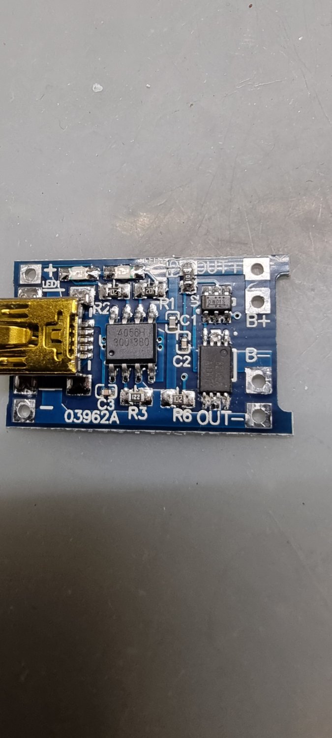
I got these TP4056 modules from an AliExpress vendor and fail to understand how the protection circuit works or if it's just typical Ali shovelware. It could be my limited understanding of electronics.

The protection circuit appears to be just for show. To the right there's a DW01S chip that prevents over charging and discharging in combination with the 8205 dual channel MOSFET.

It looks like the drain of this MOSFET isn't connected anywhere. I've tried following the traces using a multimeter and no other pin shows continuity with the drain. Source1 is connected to Battery - and Source2 is connected to Terminal -.

I suppose the Drain starts participating in the circuit when one mosfet activates.

What was the idea behind this? That the 8205 acts as an AND gate by having them both in series?

I'm trying to make an 18650 testing circuit that uses these modules to charge and discharge a battery and wanted to use the protection circuit mosfet as a trigger for discharging.

view more: next ›